Huawei said Monday at a Shanghai tech conference that it has developed a chip-design method it calls LogicFolding, which the company claims will allow it to produce semiconductors with performance equivalent to 1.4-nanometer manufacturing by 2031, the same node TSMC plans to mass-produce in 2028. He Tingbo, president of Huawei's semiconductor business, presented the work at the Institute of Electrical and Electronics Engineers' International Symposium on Circuits and Systems and said the first commercial application will be the Kirin processor inside Huawei's Mate 90 smartphone this fall.
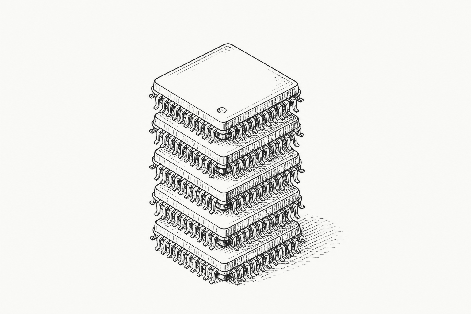
The announcement gives Beijing its most concrete claim yet that it can close a roughly three-generation gap with the West without access to ASML's extreme ultraviolet lithography machines. Instead of shrinking transistors, Huawei is stacking 2D circuits into 3D vertical structures, an approach He likened to building skyscrapers rather than widening streets. The company did not release independent performance data.
What is new today
Last Wednesday Nvidia Chief Executive Jensen Huang told CNBC his company had "largely conceded" the Chinese AI chip market to Huawei, sending Nvidia shares lower after-hours. Monday's disclosure puts an engineering roadmap behind that political reality. Huawei said it has already designed and mass-produced 381 chips over the past six years using the underlying method, which it is rebranding as the "Tau Scaling Law" — nicknamed "Her's Law" inside the Chinese tech press, after He.
China's most advanced domestic manufacturing is currently estimated at the 7-nanometer node. TSMC, which makes Nvidia's accelerators, is in volume production at 2 nanometers.
On the floor
He acknowledged the limits of the approach. Existing electronic design automation tools are not yet sufficient for full free-logic stacking, she said, and thermal management is a critical issue because vertically packed transistors trap heat. Huawei is at the start of what she described as a decade-long development path.
Participants in the room were divided on the claim. Paul Triolo of DGA Group said a folded design "can produce effective density gains, but it does not mean Huawei has solved the full process, yield, power, thermal, and device-performance problems associated with true 1.4 nm-class manufacturing." Brady Wang of Counterpoint Research told Reuters that "in the short term, China may narrow the gap with global leaders, but a technology gap with the most advanced nodes will still remain."
The reaction in Beijing
On Weibo, the hashtag #HuaweiSemiconductorFieldNewBreakthrough drew more than 40 million views by Monday afternoon, with several commenters calling it a "DeepSeek moment" for Chinese hardware. A commentary posted to an account tied to state broadcaster CCTV said competition between the U.S. and China "must be moderate and healthy, aimed at mutual advancement rather than zero-sum games."
The skeptics
The announcement leans heavily on a single keynote and company-supplied figures, with no third-party benchmarks and no public yield data. Neil Shah of Counterpoint Research said scaling LogicFolding from a flagship phone to AI datacenter accelerators would be the "ultimate litmus test for China's creative workaround to Western sanctions." Both body-tier sources for today's story lean center or lean-left; U.S. administration officials and ASML had not publicly responded to Huawei's specific 2031 timeline by press time.
The Mate 90 launch, expected in the fall, will be the first outside check on whether LogicFolding works in a shipping product.